30-pin Header
The 30-pin header is a 2 x 15 row of 2.54 mm pins along the same edge of the board as the U.2 connector. It carries GPIO, I²C, I²S, SPI, CAN, ADC, PWM and USB 2.0 signals, and 5 V and 3.3 V supply outputs. The pin table below lists what each pin carries.
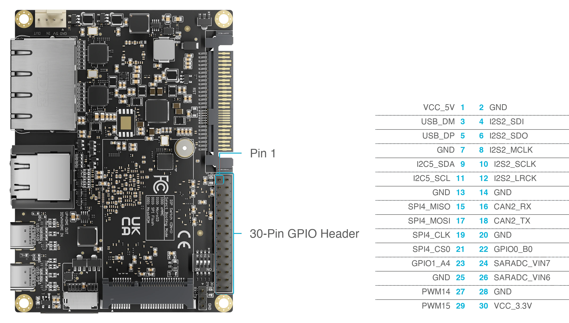
Figure 1. The 30-pin header and its pin 1
Electrical Limits
warning
- Signal pins are 3.3 V. Do not connect 5 V logic directly.
- The ADC inputs, SARADC_VIN6 (pin 26) and SARADC_VIN7 (pin 24), accept at most 1.8 V.
- The I2C5 lines have no pull-up resistors on the board. Add external pull-ups sized for the number of devices and the bus speed.
- The 5 V output (pin 1) and the 3.3 V output (pin 30) are each fused at 500 mA.
Pin Assignments
| Pin# | PinName | PinType | Input/Output | Signal Description |
|---|---|---|---|---|
| 1 | VCC_5V0 | Power | Output | Power supply for USB, 5 V output MAX 500 mA |
| 2 | GND | Power | NA | Power and signal reference ground |
| 3 | USB20_HOST0_DM | LVDS | BI | USB20 HOST Port0 Data Minus |
| 4 | I2S2_SDI_M1 | signal | Input | I2S2 data input |
| 5 | USB20_HOST0_DP | LVDS | BI | USB20 HOST Port0 Data Plus |
| 6 | I2S2_SDO_M1 | signal | Output | I2S2 data output |
| 7 | GND | Power | NA | Power and signal reference ground |
| 8 | I2S2_MCLK_M1 | signal | Output | I2S2 Master clock |
| 9 | I2C5_SDA_M3 | signal | BI | I2C5 Bus data |
| 10 | I2S2_SCLK_M1 | signal | BI | I2S2 serial clock or BCLK |
| 11 | I2C5_SCL_M3 | signal | Output | I2C5 Bus clock |
| 12 | I2S2_LRCK_M1 | signal | BI | I2S2 Left/Right channel clock |
| 13 | GND | Power | NA | Power and signal reference ground |
| 14 | GND | Power | NA | Power and signal reference ground |
| 15 | SPI4_MISO_M2 | signal | Input | SPI4 Master input, Slave output |
| 16 | CAN2_RX | signal | Input | CAN2 receive data |
| 17 | SPI4_MOSI_M2 | signal | Output | SPI4 Master output, Slave input |
| 18 | CAN2_TX | signal | Output | CAN2 transmit data |
| 19 | SPI4_CLK_M2 | signal | Output | SPI4 clock |
| 20 | GND | Power | NA | Power and signal reference ground |
| 21 | SPI4_CS0_M2 | signal | Output | SPI4 Chip Select 0 |
| 22 | GPIO0_B0 | signal | BI | GPIO bank 0 port B0 |
| 23 | GPIO1_A4 | signal | BI | GPIO bank 1 port A4 |
| 24 | SARADC_VIN7 | Analog | Input | SAR ADC Channel 7 input |
| 25 | GND | Power | NA | Power and signal reference ground |
| 26 | SARADC_VIN6 | Analog | Input | SAR ADC Channel 6 input |
| 27 | PWM14 | signal | BI | Pulse Width Modulation 14 input or output |
| 28 | GND | Power | NA | Power and signal reference ground |
| 29 | PWM15 | signal | BI | Pulse Width Modulation 15 input or output |
| 30 | VCC_3V3_S0 | Power | Output | Power supply for peripheral, 3.3 V output MAX 500 mA |