Hardware Interface
Overview
Mixtile Cluster Box is a PCIe switcher that can mount up to four Mixtile Blade 3s through PCIe interfaces, which allows for multi-node computation. Comparing with a single Blade 3 board, this powerful and versatile 4-node clustering offers boosted computing performance, faster networking, and expansive storage capacity.
The switcher consists of a backplane and a control board enclosed in a customized chassis with dual cooling fans. Thanks to the ASM2824 PCIe switch chip, the quad-channel PCIe 3.0 backplane enables seamless data transmission between Blade 3 boards for robust, uninterrupted performance.
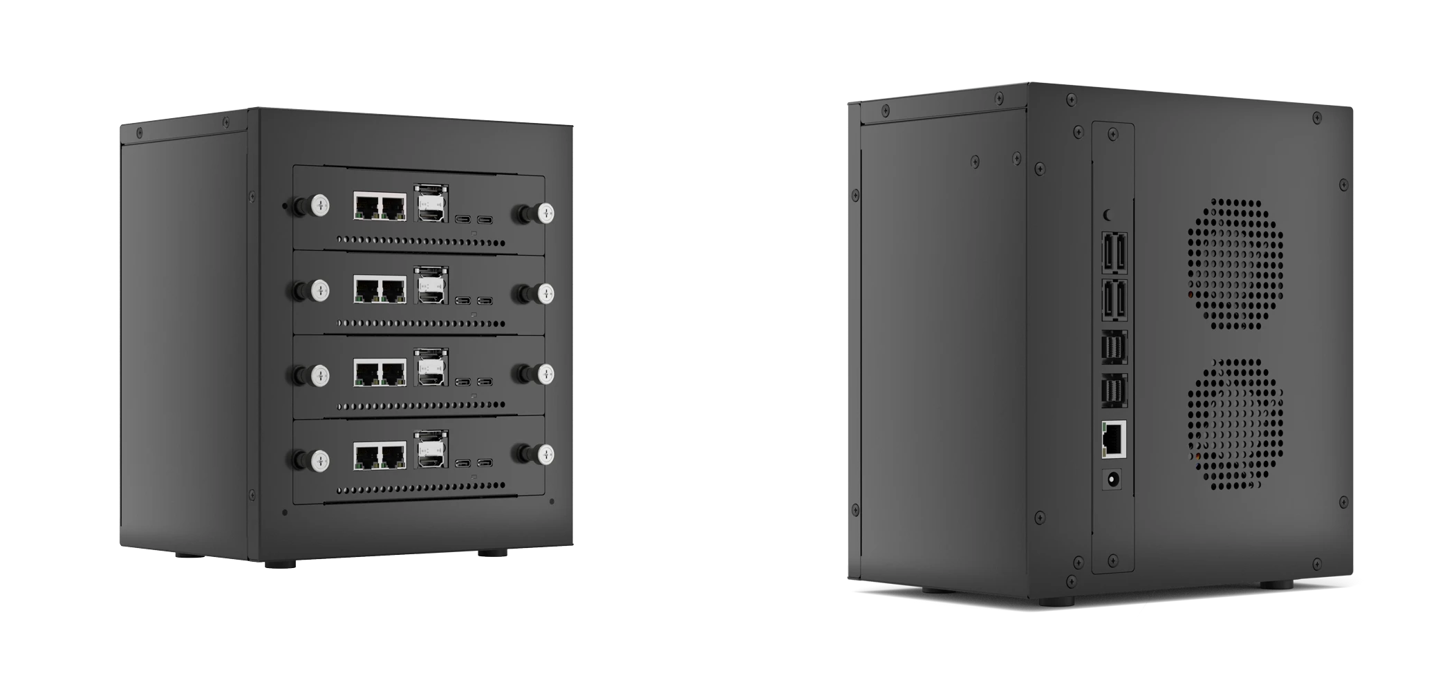
Figure 1. Cluster Box
Main features
- Boosted computational performance
A 4-node cluster enhances computational capabilities, which enables you to easily tackle complex tasks, process data-intensive applications, and accelerate your workflows.
- Seamless connectivity and uninterruptible data transmission
Driven by the ASM2824 PCIe Packet Switch chip, the cutting-edge backplane ensures seamless connectivity among Blade 3s and continuous data transmission.
- Expanded storage capacity
Four NVMe M.2 slots support PCIe 3.0 x2, which are fully compatible with SSDs. You can scale out storage without compromising on storing critical data or large-scale projects.
- Compact size with efficient cooling system
A customized small chassis equipped with two internal 60 mm fans ensures that your system runs stably and smoothly in a very small format.
Technical specifications
| Item | Specification |
|---|---|
| Switch | ASMedia ASM2824, support four PCIe 3.0 4-lane ports |
| Storage interfaces | 4x NVMe M.2 M-Key slot (PCIe 3.0 x2 each slot, connecting to Blade 3) 4x SATA 3.0 port (connecting to Blade 3) |
| Connectivity | 4x U.2 interfaces (connecting to Blade 3) |
| Network | 1x 100/1000 Mbps Ethernet port |
| PCIe expansion | 2x SFF-8643 port (support PCIe 3.0 x4 each, upstream) |
| Fan | 2x 60 mm fans |
| Software support | Preloaded customized Linux system and Kubernetes |
| Power | 1x DC jack port, 19~19.5 V 4.74 A power input Power button with a blue LED indicator |
| Material | Metal case, SGCC steel |
| Dimensions | 213 mm x 190 mm x 129 mm |
| Temperature | Operating: 0°C to 80°C Storage: -20°C to 85°C |
| Relative humidity | Operating: 10% to 90% Storage: 5% to 95% |
Table 1. Technical specifications of Cluster Box
Functional description
Microcontroller
MediaTek MT7620A router-on-a-chip
- Embedded MIPS24KEc (580 MHz) with 64 KB I-Cache and 32 KB D-Cache
- 256 Mbytes DDR2
- 16 Mbytes SPI Flash
- Firmware: OpenWrt System
Switch
ASM2824 PCIe Packet switch
- Upstream PCIe interface
- 1-, 2-, 4-, or 8-lane PCIe® connecting with root port
- Automatic detection of lane configuration on boot-up
- Supporting transfer rate of 2.5 GT/s (250 MB/s), 5 GT/s (500 MB/s), and 8 GT/s (985 MB/s) per lane
- Downstream PCIe interface
- 16 lane PCIe® 3.1 interface supporting up to 12 PCIe® ports
- Support L0s/L1/L23/L3 power saving states
- Support L1 substate deep power saving mode
- Support wake up function in S3/S4
- Support port disable by individual control
- Support LTR
- Support AER
- Support SRIS on both upstream and downstream ports.
- Max Payload Size = 512 Byte
- Support hot-plug, surprise remove
Connectivity
U.2 interface
The U.2 interface employs a 68-pin U.2 connector with a standard SATA signal, a SATA 3.0 signal, a PCIe 3.0 X4 signal (four lanes PCIe 3.0), and 12 V or 19 V power output for main board.
| Pin # | Pin name | Signal description | Direction | Pin type |
|---|---|---|---|---|
| 2 | SATA_TXP | SATA Transmit+ | Output | SATA PHY |
| 3 | SATA_TXN | SATA Transmit- | Output | SATA PHY |
| 5 | SATA_RXN | SATA Receive- | Input | SATA PHY |
| 6 | SATA_RXP | SATA Receive+ | Input | SATA PHY |
| 8 | PCIE30_PORT1_REFCLKP | PCIE3.0 Reference Clock1+ | Input | PCIe PHY |
| 9 | PCIE30_PORT1_REFCLKN | PCIE3.0 Reference Clock1– | Input | PCIe PHY |
| 11 | PCIE30X4_CLKREQN | PCIE3.0 Clock Request | Bidir | Open Drain–3.3V |
| 12 | PCIE30X4_PERSTN | PCIE3.0 Reset | Bidir | Open Drain–3.3V |
| 14 | PCIE30X4_WAKEN | PCIE3.0 Wake | Input | Open Drain–3.3V |
| 17 | M.2_DET | M.2 Plug Detect | Input | Open Drain–3.3V |
| 22 | LED | LED Power | Input | Power |
| 23 | PRZ | GPIO | Bidir | CMOS–3.3V |
| 26 | 19V | 19V main Power | Output | Power |
| 27 | 19V | 19V Main Power | Output | Power |
| 28 | 19V | 19V Main Power | Output | Power |
| 33 | PCIE30_PORT0_TX3P | PCIe3.0 Transmit 3+ | Output | PCIe PHY |
| 34 | PCIE30_PORT0_TX3N | PCIe3.0 Transmit 3– | Output | PCIe PHY |
| 36 | PCIE30_PORT0_RX3N | PCIe3.0 Receive 3– | Input | PCIe PHY |
| 37 | PCIE30_PORT0_RX3P | PCIe3.0 Receive 3+ | Input | PCIe PHY |
| 39 | PCIE30_PORT0_TX2P | PCIe3.0 Transmit 2+ | Output | PCIe PHY |
| 40 | PCIE30_PORT0_TX2N | PCIe3.0 Transmit 2– | Output | PCIe PHY |
| 42 | PCIE30_PORT0_RX2N | PCIe3.0 Receive 2– | Input | PCIe PHY |
| 43 | PCIE30_PORT0_RX2P | PCIe3.0 Receive 2+ | Input | PCIe PHY |
| 45 | PCIE30_PORT0_TX1P | PCIe3.0 Transmit 1+ | Output | PCIe PHY |
| 46 | PCIE30_PORT0_TX1N | PCIe3.0 Transmit 1– | Output | PCIe PHY |
| 48 | PCIE30_PORT0_RX1N | PCIe3.0 Receive 1– | Input | PCIe PHY |
| 49 | PCIE30_PORT0_RX1P | PCIe3.0 Receive 1+ | Input | PCIe PHY |
| 51 | POWER_ON | MB Power on control GPIO | Bidir | Open Drain–3.3V |
| 56 | UART_TXD | UART Transmit | Output | CMOS–3.3V |
| 57 | UART_RXD | UART Receive | Input | CMOS–3.3V |
| 59 | RESET | MB Reset control GPIO | Bidir | Open Drain–3.3V |
| 61 | PCIE30_PORT0_TX0P | PCIe3.0 Transmit 0+ | Output | PCIe PHY |
| 62 | PCIE30_PORT0_TX0N | PCIe3.0 Transmit 0– | Output | PCIe PHY |
| 64 | PCIE30_PORT0_RX0N | PCIe3.0 Receive 0– | Input | PCIe PHY |
| 65 | PCIE30_PORT0_RX0P | PCIe3.0 Receive 0+ | Input | PCIe PHY |
| 67 | DPE_CLKN0 | PCIE3.0 Reference Clock0– | Input | PCIe PHY |
| 68 | DPE_CLKP0 | PCIE3.0 Reference Clock0+ | Input | PCIe PHY |
Table 2. U.2 pin descriptions
M.2 interface
The M.2 interface employs a 75-position M.2 connector with a standard PCIE3.0 X2 signal, and for PCIE Module 3.3 V power Output. It can be used for external SSD to increase storage capacity.
| Pin # | Pin name | Signal description | Direction | Pin type |
|---|---|---|---|---|
| 3 | M.2_DET | M.2 Plug Detect | Input | Open Drain–3.3V |
| 29 | M2_PCIE30_PORT0_RX1N | PCIe3.0 Receive 1– | Input | PCIe PHY |
| 31 | M2_PCIE30_PORT0_RX1P | PCIe3.0 Receive 1+ | Input | PCIe PHY |
| 35 | M2_PCIE30_PORT0_TX1N | PCIe3.0 Transmit 1- | Output | PCIe PHY |
| 37 | M2_PCIE30_PORT0_TX1P | PCIe3.0 Transmit 1+ | Output | PCIe PHY |
| 41 | M2_PCIE30_PORT0_RX0N | PCIe3.0 Receive 0– | Input | PCIe PHY |
| 43 | M2_PCIE30_PORT0_RX0P | PCIe3.0 Receive 0+ | Input | PCIe PHY |
| 47 | M2_PCIE30_PORT0_TX0N | PCIe3.0 Transmit 0- | Output | PCIe PHY |
| 49 | M2_PCIE30_PORT0_TX0P | PCIe3.0 Transmit 0+ | Output | PCIe PHY |
| 53 | PCIE30_PORT1_REFCLKN | PCIE3.0 Reference Clock1– | Input | PCIe PHY |
| 55 | PCIE30_PORT1_REFCLKP | PCIE3.0 Reference Clock1+ | Input | PCIe PHY |
| 2 | VCC3V3_PCIE | 3.3V M.2 Module Power | Output | Power |
| 4 | VCC3V3_PCIE | 3.3V M.2 Module Power | Output | Power |
| 12 | VCC3V3_PCIE | 3.3V M.2 Module Power | Output | Power |
| 14 | VCC3V3_PCIE | 3.3V M.2 Module Power | Output | Power |
| 16 | VCC3V3_PCIE | 3.3V M.2 Module Power | Output | Power |
| 18 | VCC3V3_PCIE | 3.3V M.2 Module Power | Output | Power |
| 50 | PCIE30X4_PERSTn | PCIE3.0 Reset | Bidir | Open Drain–3.3V |
| 52 | PCIE30X4_CLKREQn | PCIE3.0 Clock Request | Bidir | Open Drain–3.3V |
| 54 | PCIE30X4_WAKEN | PCIE3.0 Wake | Input | Open Drain–3.3V |
| 70 | VCC3V3_PCIE | 3.3V M.2 Module Power | Output | Power |
| 72 | VCC3V3_PCIE | 3.3V M.2 Module Power | Output | Power |
| 74 | VCC3V3_PCIE | 3.3V M.2 Module Power | Output | Power |
Table 3. M.2 pin descriptions
100/1000 Mbps Ethernet controller
- Support two identical Ethernet controllers
- Support 10/100/1000 Mbps data transfer rates with the RGMII interface
- Support 10/100 Mbps data transfer rates with the RMII interfaces
- Support both full-duplex and half-duplex operation
- Supports IEEE 802.1Q VLAN tag detection for reception frames
- Support detection of LAN wake-up frames and AMD Magic Packet frames
- Support checking IPv4 header checksum and TCP, UDP, or ICMP checksum encapsulated in IPv4 or IPv6 datagram
- Support for TCP Segmentation Offload (TSO) and UDP Fragmentation Offload (UFO)
SATA interface
- Compatible with Serial SATA 3.3 and AHCI Revision 1.3.1
- Support 1.5 Gb/s, 3.0 Gb/s, 6.0 Gb/s
- The Cluster Box provides four SATA connections associated with the Blade 3 nodes.
SFF-8643
- Compliant with the latest SAS 3.0 spec, and supports 12 Gb/s data transfer protocol
- Support up to 4-ports (4 lanes) of SAS data.
| Pin # | Pin name | Signal description | Direction | Pin type |
|---|---|---|---|---|
| A1 | CLK0P_8643 | SFF-8643 SAS Reference Clock+ | Output | PCIe PHY |
| A2 | CLK0N_8643 | SFF-8643 SAS Reference Clock- | Output | PCIe PHY |
| A4 | UPE_RXP1 | SFF-8643 SAS Receive 1+ | Input | PCIe PHY |
| A5 | UPE_RXN1 | SFF-8643 SAS Receive 1- | Input | PCIe PHY |
| A7 | UPE_RXP3 | SFF-8643 SAS Receive 3+ | Input | PCIe PHY |
| A8 | UPE_RXN3 | SFF-8643 SAS Receive 3- | Input | PCIe PHY |
| C1 | USB_IN_DP | USB2.0 data+ | Bidir | USB PHY |
| C2 | USB_IN_DM | USB2.0 data- | Bidir | USB PHY |
| C4 | UPE_TXP1 | SFF-8643 SAS Transmit 1+ | Output | PCIe PHY |
| C5 | UPE_TXN1 | SFF-8643 SAS Transmit 1- | Output | PCIe PHY |
| C7 | UPE_TXP3 | SFF-8643 SAS Transmit 3+ | Output | PCIe PHY |
| C8 | UPE_TXN3 | SFF-8643 SAS Transmit 3- | Output | PCIe PHY |
| B1 | 8643_RESET | SFF-8643 Reset control | Bidir | Open Drain–3.3V |
| B2 | 8643_SEL | SFF-8643 SEL GPIO | Bidir | CMOS–3.3V |
| B4 | 8643_RXP0 | SFF-8643 SAS Receive 0+ | Input | PCIe PHY |
| B5 | 8643_RXN0 | SFF-8643 SAS Receive 0- | Input | PCIe PHY |
| B7 | UPE_RXP2 | SFF-8643 SAS Receive 2+ | Input | PCIe PHY |
| B8 | UPE_RXN2 | SFF-8643 SAS Receive 2- | Input | PCIe PHY |
| D4 | 8643_TXP0 | SFF-8643 SAS Transmit 0+ | Output | PCIe PHY |
| D5 | 8643_TXN0 | SFF-8643 SAS Transmit 0- | Output | PCIe PHY |
| D7 | UPE_TXP2 | SFF-8643 SAS Transmit 2+ | Output | PCIe PHY |
| D8 | UPE_TXN2 | SFF-8643 SAS Transmit 2- | Output | PCIe PHY |
Table 4. SFF-8643 pin descriptions
UART
The leading connector for system DEBUG.
| Pin # | Pin Name | Signal Description | Direction | Pin Type |
|---|---|---|---|---|
| 1 | UART_RX | UART Receive | Input | CMOS–3.3V |
| 2 | UART_TX | UART Transmit | Output | CMOS–3.3V |
| 3 | GND | GND | – | Power |
Table 5. UART pin descriptions
Block diagram
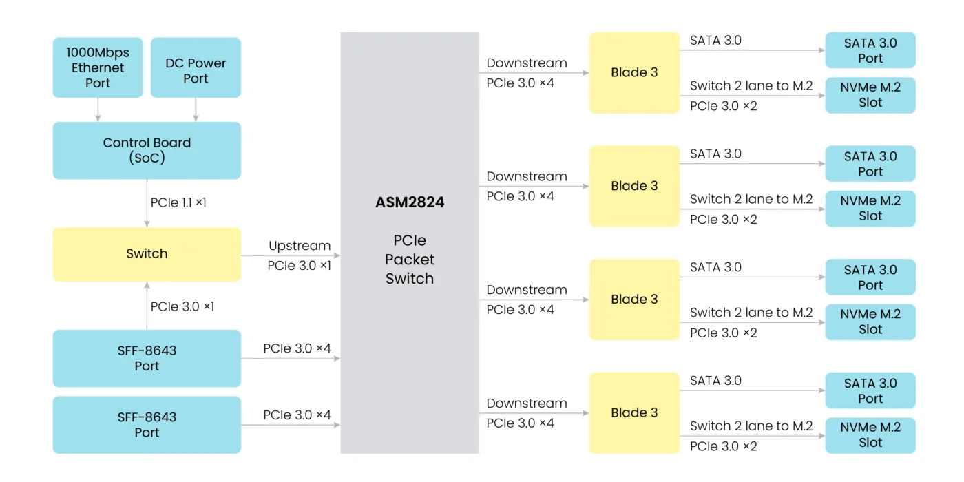
Figure 2. Block diagram of Cluster Box
Technical support
MIXTILE technical support team assists you with the questions you may have. Contact us with the following methods below.
- Email: support@mixtile.com
- Website: https://www.mixtile.com
- Community: https://community.mixtile.com/