Display and Camera Connectors
Besides HDMI, Edge 2 has four FPC connectors for displays and a camera, all on the bottom side of the board:
| Connector | Pins | Use |
|---|---|---|
| eDP | 30 | eDP panel, with backlight power and control |
| MIPI-DSI0 | 30 | MIPI DSI panel, with touch-panel I²C and control signals |
| MIPI-DSI1 | 30 | Second MIPI DSI panel, with touch-panel I²C and control signals |
| MIPI-CSI | 40 | MIPI CSI camera module |
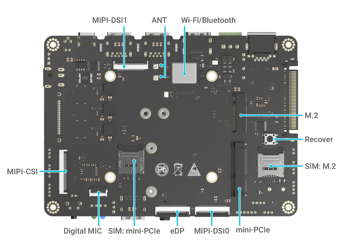
Figure 1. The display and camera connectors, on the bottom side
Using these connectors needs a panel or camera module and support for it in the operating system. For the status in Mixtile OS, see Hardware Interfaces in Mixtile OS.
Electrical Notes
- The eDP connector supplies 12 V on pins 28 to 30 for the panel backlight, and 3.3 V on pins 16 and 17.
- The MIPI-DSI and MIPI-CSI connectors supply 5 V on pins 28 to 30, up to 500 mA per connector.
- Both MIPI-DSI connectors share one touch-panel I²C bus, I2C1, and the touch interrupt and reset lines.
Pin Assignments
eDP
| Pin# | PinName | PinType | Input/Output | Signal Description |
|---|---|---|---|---|
| 1 | GND | GND | NA | Power and signal reference ground |
| 2 | EDP_TX_D1N | LVDS | Output | EDP data signal Negative |
| 3 | EDP_TX_D1P | LVDS | Output | EDP data signal Positive |
| 4 | GND | GND | NA | Power and signal reference ground |
| 5 | EDP_TX_D0N | LVDS | Output | EDP data signal Negative |
| 6 | EDP_TX_D0P | LVDS | Output | EDP data signal Positive |
| 7 | GND | GND | NA | Power and signal reference ground |
| 8 | EDP_TX_AUXN_CON | LVDS | Output | EDP clock signal Negative |
| 9 | EDP_TX_AUXP_CON | LVDS | Output | EDP clock signal Positive |
| 10 | GND | GND | NA | Power and signal reference ground |
| 11 | EDP_TX_D2N | LVDS | Output | EDP data signal Negative |
| 12 | EDP_TX_D2P | LVDS | Output | EDP data signal Positive |
| 13 | GND | GND | NA | Power and signal reference ground |
| 14 | EDP_TX_D3N | LVDS | Output | EDP data signal Negative |
| 15 | EDP_TX_D3P | LVDS | Output | EDP data signal Positive |
| 16 | 3.3V | PWR | Output | 3.3V @ 500mA Max in total |
| 17 | 3.3V | PWR | Output | 3.3V @ 500mA Max in total |
| 18 | GND | GND | NA | Power and signal reference ground |
| 19 | GND | GND | NA | Power and signal reference ground |
| 20 | EDP_HPD_GPIO0_C2 | IO | Input | eDP hot plug detect signal |
| 21 | GND | GND | NA | Power and signal reference ground |
| 22 | GND | GND | NA | Power and signal reference ground |
| 23 | GND | GND | NA | Power and signal reference ground |
| 24 | GND | GND | NA | Power and signal reference ground |
| 25 | EDP_BL_EN_GPIO3_C1 | IO | Output | Output for enable backlight power |
| 26 | EDP_PWM12_GPIO4_C5 | IO | Output | PWM Output for backlight adjust |
| 27 | GND | GND | NA | Power and signal reference ground |
| 28 | 12V | PWR | Output | 12V power supply for backlight |
| 29 | 12V | PWR | Output | 12V power supply for backlight |
| 30 | 12V | PWR | Output | 12V power supply for backlight |
MIPI-DSI0
| Pin# | PinName | PinType | Input/Output | Signal Description |
|---|---|---|---|---|
| 1 | GND | GND | NA | Power and signal reference ground |
| 2 | MIPI_DSI_TX0_D0N | LVDS | Output | MIPI-DSI0 data signal Negative |
| 3 | MIPI_DSI_TX0_D0P | LVDS | Output | MIPI-DSI0 data signal Positive |
| 4 | GND | GND | NA | Power and signal reference ground |
| 5 | MIPI_DSI_TX0_D1N | LVDS | Output | MIPI-DSI0 data signal Negative |
| 6 | MIPI_DSI_TX0_D1P | LVDS | Output | MIPI-DSI0 data signal Positive |
| 7 | GND | GND | NA | Power and signal reference ground |
| 8 | MIPI_DSI_TX0_CLKN | LVDS | Output | MIPI-DSI0 clock signal Negative |
| 9 | MIPI_DSI_TX0_CLKP | LVDS | Output | MIPI-DSI0 clock signal Positive |
| 10 | GND | GND | NA | Power and signal reference ground |
| 11 | MIPI_DSI_TX0_D2N | LVDS | Output | MIPI-DSI0 data signal Negative |
| 12 | MIPI_DSI_TX0_D2P | LVDS | Output | MIPI-DSI0 data signal Positive |
| 13 | GND | GND | NA | Power and signal reference ground |
| 14 | MIPI_DSI_TX0_D3N | LVDS | Output | MIPI-DSI0 data signal Negative |
| 15 | MIPI_DSI_TX0_D3P | LVDS | Output | MIPI-DSI0 data signal Positive |
| 16 | GND | GND | NA | Power and signal reference ground |
| 17 | LCD0_BL_PWM4 | IO | Output | PWM Output for backlight adjust |
| 18 | NC | NA | NA | Not connected to this pin |
| 19 | 3.3V | PWR | Output | 3.3V @ 200mA Max |
| 20 | LCD0_RST_L_GPIO1_D1 | IO | Output | GPIO output for lcd reset |
| 21 | SARADC_VIN2_LCD_ID | ANA | Input | Analog signal Input |
| 22 | LCD0_PWREN_H_GPIO0_C7 | IO | Output | GPIO output for lcd power on |
| 23 | I2C1_SCL_TP | IO | Output | I2C clock signal for touch panel |
| 24 | I2C1_SDA_TP | IO | I/O | I2C data signal for touch panel |
| 25 | TP_INT_L_GPIO0_B5 | IO | Input | GPIO for touch panel interrupt |
| 26 | TP_RST_L_GPIO0_B6 | IO | Output | GPIO for touch panel reset |
| 27 | GND | GND | NA | Power and signal reference ground |
| 28 | 5V | PWR | Output | 5V @ 500mA Max in total |
| 29 | 5V | PWR | Output | 5V @ 500mA Max in total |
| 30 | 5V | PWR | Output | 5V @ 500mA Max in total |
MIPI-DSI1
| Pin# | PinName | PinType | Input/Output | Signal Description |
|---|---|---|---|---|
| 1 | GND | GND | NA | Power and signal reference ground |
| 2 | MIPI_DSI_TX1_D0N | LVDS | Output | MIPI-DSI1 data signal Negative |
| 3 | MIPI_DSI_TX1_D0P | LVDS | Output | MIPI-DSI1 data signal Positive |
| 4 | GND | GND | NA | Power and signal reference ground |
| 5 | MIPI_DSI_TX1_D1N | LVDS | Output | MIPI-DSI1 data signal Negative |
| 6 | MIPI_DSI_TX1_D1P | LVDS | Output | MIPI-DSI1 data signal Positive |
| 7 | GND | GND | NA | Power and signal reference ground |
| 8 | MIPI_DSI_TX1_CLKN | LVDS | Output | MIPI-DSI1 clock signal Negative |
| 9 | MIPI_DSI_TX1_CLKP | LVDS | Output | MIPI-DSI1 clock signal Positive |
| 10 | GND | GND | NA | Power and signal reference ground |
| 11 | MIPI_DSI_TX1_D2N | LVDS | Output | MIPI-DSI1 data signal Negative |
| 12 | MIPI_DSI_TX1_D2P | LVDS | Output | MIPI-DSI1 data signal Positive |
| 13 | GND | GND | NA | Power and signal reference ground |
| 14 | MIPI_DSI_TX1_D3N | LVDS | Output | MIPI-DSI1 data signal Negative |
| 15 | MIPI_DSI_TX1_D3P | LVDS | Output | MIPI-DSI1 data signal Positive |
| 16 | GND | GND | NA | Power and signal reference ground |
| 17 | PWM5 | IO | Output | PWM Output for backlight adjust |
| 18 | NC | NA | NA | Not connected to this pin |
| 19 | 3.3V | PWR | Output | 3.3V @ 200mA Max |
| 20 | LCD1_RST_L_GPIO3_B6 | IO | Output | GPIO output for lcd reset |
| 21 | SARADC_VIN2_LCD_ID | ANA | Input | Analog signal Input |
| 22 | LCD1_PWREN_H_GPIO4_D2 | IO | Output | GPIO output for lcd power enable |
| 23 | I2C1_SCL_TP | IO | Output | I2C clock signal for touch panel |
| 24 | I2C1_SDA_TP | IO | I/O | I2C data signal for touch panel |
| 25 | TP_INT_L_GPIO0_B5 | IO | Input | GPIO for touch panel interrupt |
| 26 | TP_RST_L_GPIO0_B6 | IO | Output | GPIO for touch panel reset |
| 27 | GND | GND | NA | Power and signal reference ground |
| 28 | 5V | PWR | Output | 5V @ 500mA Max in total |
| 29 | 5V | PWR | Output | 5V @ 500mA Max in total |
| 30 | 5V | PWR | Output | 5V @ 500mA Max in total |
MIPI-CSI
| Pin# | PinName | PinType | Input/Output | Signal Description |
|---|---|---|---|---|
| 1 | GND | GND | NA | Power and signal reference ground |
| 2 | MIPI_CSI_RX_D0N | LVDS | Input | MIPI_CSI data signal Negative |
| 3 | MIPI_CSI_RX_D0P | LVDS | Input | MIPI_CSI data signal Positive |
| 4 | GND | GND | NA | Power and signal reference ground |
| 5 | MIPI_CSI_RX_D1N | LVDS | Input | MIPI_CSI data signal Negative |
| 6 | MIPI_CSI_RX_D1P | LVDS | Input | MIPI_CSI data signal Positive |
| 7 | GND | GND | NA | Power and signal reference ground |
| 8 | MIPI_CSI_RX_CLK0N | LVDS | Input | MIPI_CSI clock signal Negative |
| 9 | MIPI_CSI_RX_CLK0P | LVDS | Input | MIPI_CSI clock signal Positive |
| 10 | GND | GND | NA | Power and signal reference ground |
| 11 | MIPI_CSI_RX_D2N | LVDS | Input | MIPI_CSI data signal Negative |
| 12 | MIPI_CSI_RX_D2P | LVDS | Input | MIPI_CSI data signal Positive |
| 13 | GND | GND | NA | Power and signal reference ground |
| 14 | MIPI_CSI_RX_D3N | LVDS | Input | MIPI_CSI data signal Negative |
| 15 | MIPI_CSI_RX_D3P | LVDS | Input | MIPI_CSI data signal Positive |
| 16 | GND | GND | NA | Power and signal reference ground |
| 17 | CIF_CLKOUT | IO | Output | CLOCK output for camera |
| 18 | GND | GND | NA | Power and signal reference ground |
| 19 | NC | NA | NA | Not connected to this pin |
| 20 | CAMERA0_RST_L_GPIO4_B5 | IO | Output | GPIO output for camera reset |
| 21 | CAMERA0_PDN_L_GPIO4_B4 | IO | Output | GPIO output for camera disable |
| 22 | CAMERA0_PWREN_GPIO1_D4 | IO | Output | GPIO output for camera enable |
| 23 | I2C4_SCL_M0 | IO | Output | I2C clock signal |
| 24 | I2C4_SDA_M0 | IO | Input | I2C data signal |
| 25 | PWM14_M0 | IO | Output | PWM Output signal |
| 26 | GND | GND | NA | Power and signal reference ground |
| 27 | GND | GND | NA | Power and signal reference ground |
| 28 | 5V | PWR | Output | 5V @ 500mA Max in total |
| 29 | 5V | PWR | Output | 5V @ 500mA Max in total |
| 30 | 5V | PWR | Output | 5V @ 500mA Max in total |
| 31 | GND | GND | NA | Power and signal reference ground |
| 32 | NC | NA | NA | Not connected to this pin |
| 33 | NC | NA | NA | Not connected to this pin |
| 34 | NC | NA | NA | Not connected to this pin |
| 35 | GND | GND | NA | Power and signal reference ground |
| 36 | MIPI_MCLK1 | IO | Output | CLOCK output for camera |
| 37 | GND | GND | NA | Power and signal reference ground |
| 38 | MIPI_CSI_RX_CLK1N | LVDS | Input | MIPI_CSI clock signal Negative |
| 39 | MIPI_CSI_RX_CLK1P | LVDS | Input | MIPI_CSI clock signal Positive |
| 40 | GND | GND | NA | Power and signal reference ground |