Other Connectors
This page covers the smaller connectors on the top side of the board.
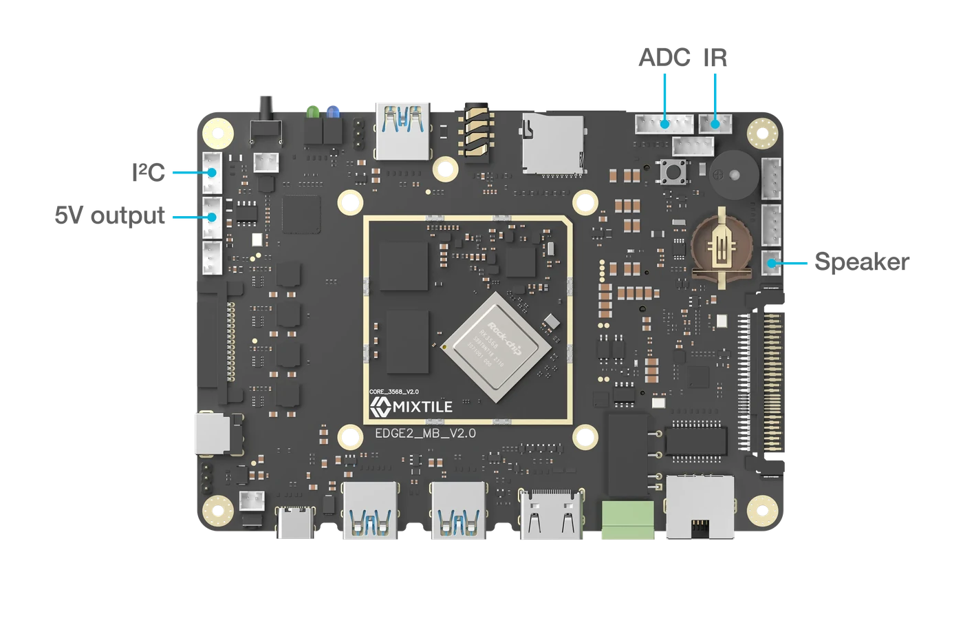
Figure 1. The I²C, 5V output, ADC, IR and speaker connectors
For the S/PDIF, digital microphone, power button and reset button connectors, see the labelled board views in Hardware Information.
For how Mixtile OS exposes these connectors, see Hardware Interfaces in Mixtile OS.
I²C
A four-pin connector on the left edge, with 3.3 V signals and 4.7 kΩ pull-up resistors on the board. It carries I2C3 of the SoC, which is shared with the on-board real-time clock at address 0x51, so do not connect a device with the same address.
| Pin# | PinName | PinType | Input/Output | Signal Description |
|---|---|---|---|---|
| 1 | 3.3V | PWR | Output | 3.3V @ 100mA Max |
| 2 | I2C3_SCL | IO | Output | I2C clock signal |
| 3 | I2C3_SDA | IO | I/O | I2C data signal |
| 4 | GND | GND | NA | Power and signal reference ground |
ADC
A six-pin connector on the top edge, with four inputs, channels 4 to 7, to the SoC's 10-bit SAR ADC. The ADC reference is 1.8 V, so an input voltage above 1.8 V cannot be measured.
| Pin# | PinName | PinType | Input/Output | Signal Description |
|---|---|---|---|---|
| 1 | 3.3V | PWR | Output | 3.3V @ 100mA Max |
| 2 | SARADC_VIN4 | ANA | Input | ADC analog signal |
| 3 | SARADC_VIN5 | ANA | Input | ADC analog signal |
| 4 | SARADC_VIN6 | ANA | Input | ADC analog signal |
| 5 | SARADC_VIN7 | ANA | Input | ADC analog signal |
| 6 | GND | GND | NA | Power and signal reference ground |
IR
A connector on the top edge for an infrared receiver, wired to PWM7 of the SoC.
5V Output
A four-pin connector on the left edge that supplies 5 V to external devices, up to 2 A in total.
| Pin# | PinName | PinType | Input/Output | Signal Description |
|---|---|---|---|---|
| 1 | 5V | PWR | Output | 5V @ 2A Max in total |
| 2 | 5V | PWR | Output | 5V @ 2A Max in total |
| 3 | GND | GND | NA | Power and signal reference ground |
| 4 | GND | GND | NA | Power and signal reference ground |
Speaker
A two-pin connector on the right edge for a speaker, driven by the audio codec of the RK809 power-management chip.
| Pin# | PinName | PinType | Input/Output | Signal Description |
|---|---|---|---|---|
| 1 | SPK+ | ANA | Output | Speaker driver output Positive |
| 2 | SPK- | ANA | Output | Speaker driver output Negative |
S/PDIF
A three-pin connector on the left edge.
| Pin# | PinName | PinType | Input/Output | Signal Description |
|---|---|---|---|---|
| 1 | SPDIF_TX | IO | Output | SPDIF output signal |
| 2 | 3.3V | PWR | Output | 3.3V @ 100mA Max |
| 3 | GND | GND | NA | Power and signal reference ground |
Digital Microphone
A ten-pin connector on the bottom side of the board, marked Digital MIC, for PDM microphones.
| Pin# | PinName | PinType | Input/Output | Signal Description |
|---|---|---|---|---|
| 1 | 3.3V | PWR | Output | 3.3V @ 500mA Max in total |
| 2 | 3.3V | PWR | Output | 3.3V @ 500mA Max in total |
| 3 | GND | GND | NA | Power and signal reference ground |
| 4 | GND | GND | NA | Power and signal reference ground |
| 5 | PDM_SDI1 | IO | Input | PDM data signal |
| 6 | PDM_SDI2 | IO | Input | PDM data signal |
| 7 | PDM_SDI3 | IO | Input | PDM data signal |
| 8 | GND | GND | NA | Power and signal reference ground |
| 9 | PDM_CLK1 | IO | Output | PDM clock signal |
| 10 | GND | GND | NA | Power and signal reference ground |
Power and Reset Button Connectors
Two two-pin connectors for external buttons, for example on a custom enclosure. Shorting a connector's pin 1 to GND has the same effect as pressing the button on the board.
Power button connector
| Pin# | PinName | PinType | Input/Output | Signal Description |
|---|---|---|---|---|
| 1 | PWRON_CON | IO | Input | Active-low, same as PWR button |
| 2 | GND | GND | NA | Power and signal reference ground |
Reset button connector
| Pin# | PinName | PinType | Input/Output | Signal Description |
|---|---|---|---|---|
| 1 | RESET_KEY | IO | Input | Active-low reset signal, same as RESET button |
| 2 | GND | GND | NA | Power and signal reference ground |